Review of HackerBox 0121 - MCU Lab 2025
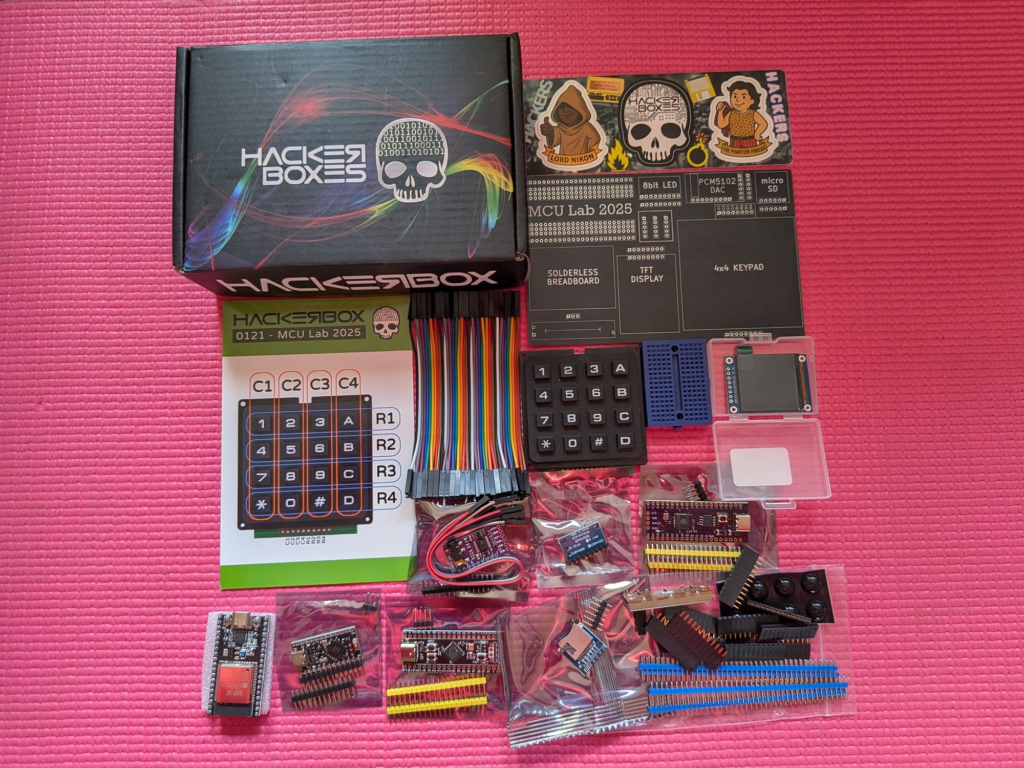
This is my review of HackerBox #0121 - MCU Lab 2025. See the HackerBox tag for my other reviews. The instructions for the kit are available on Instructables as usual. The MCU Lab 2025 is a remix of HackerBox 0051 - The MCU Lab from 2019.
The box actually arrived early this time, but I was busy attempting to install Jellyfin on Tizen at my inlaws around Thanksgiving and then off at NeurIPS 2025 in San Diego. Now I've finally had some time to wrap up the box and do a write up.
This month involves working with four different micro controllers:
- Ultimate Pico RP2040 16MB Development Board
- ESP-WROOM-32 Development Board
- STM32F401CCU6 Black Pill Development Board
- NRF52840 SuperMini Development Board
Which is pretty exciting because I have not worked with an STM nor Nordic board yet. As I mentioned in my post on learning Rust, its a good time to have other options than the Arduino ecosystem, considering the Qualcomm acquisition.
Comparing the four MCUs
The guide starts with a nice video comparing the for microcontroller options the kit provides. In the ESP32 section he describes the chip as a "wireless powerhouse". Its nice to hear an affirmation about using that chip in my ESP32 WiFi and BLE wardriving scanner prototype.
Also, I hadn't known that you need to get FCC approval if you want to ship a product using a bare chip ESP32. Sparkfun made a guide about the process, but it seems to have disappeared this year. I found a copy from 2024 in the wayback machine.
Now the trade off of course for the ESP32 is the higher power draw. The STM32 and the NRF52 can work better for low and ultra low power use cases. The RP2040 is a nice affordable option, though I hadn't realized there is no internal flash.
Outside of the video, the written guide provides an overview of all four development boards and directions on configuring the Arduino IDE.
Back with the ESP32 and RP2040 again
The ESP32 and RPi chip sections were very familiar.
The ESP32 dev board is the same one I tried out in box #0191 - Geopositioning. The guide had me run the WifiScan sketch example from the Arduino IDE examples just like in box 0191. This is also the same sketch I used in my wardriving prototype.
RP2040 is the chip the Raspberry Pi Pico is built off, which was used in box #0118 - More Human. However, this time I got to play around with CircuitPython! The guide had me do a simple blink sketch, but I would love to play with CircuitPython more in the future for quick prototypes. Oh and the guide also had me setup and use the Arduino blink sketch.
New experiments with the STM32F401CCU6
The chip's description notes there are specific instructions for DSP. If I ever get back to HRV processing, I wonder if these chips can be used for the signal processing.
Anyways, the guide had me set up the Arduino IDE by adding the chip support. They didn't instruct me to run any specific sketch, so I did the classic blink to verify everything works.
They also linked to a guide for using MicroPython. A second framework for embedded Python? Not quite. Adafruit has an article explaining that CircuitPython is a fork of MicroPython designed to be a little easier to use. The CircuitPython documentation details the full set of differences. Also, some quick searching showa that MicroPython would also work on the RP2040, but CircuitPython does not seem to support the STM32F401CCU6 [1]
Sniffing with the nRF52840
Now this is a cool chip. The nRF52840 supports both Zigbee and Thread which would be fun to use in a home automation project. Even less common than that is the Ant+ support! Maybe I could mess around with my SmartSpin2k, or other fitness sensors that use the protocol.
The guide had me try out the nRF Sniffer project using an Adafruit tutorial and work with Wireshark. Interestingly enough the process starts by loading the Adafruit nRF52 Bootloader firmware on the device. Then I loaded Nordics nRF sniffer which seems to be closed source.
This is fortuitous, since I have project on the back burner to reverse the BLE protocol for my water bottle [2] and add support to Gadgetbridge. So many project ideas, so little time.
Oh, also CirtuitPython supports the nRF52840 as well.
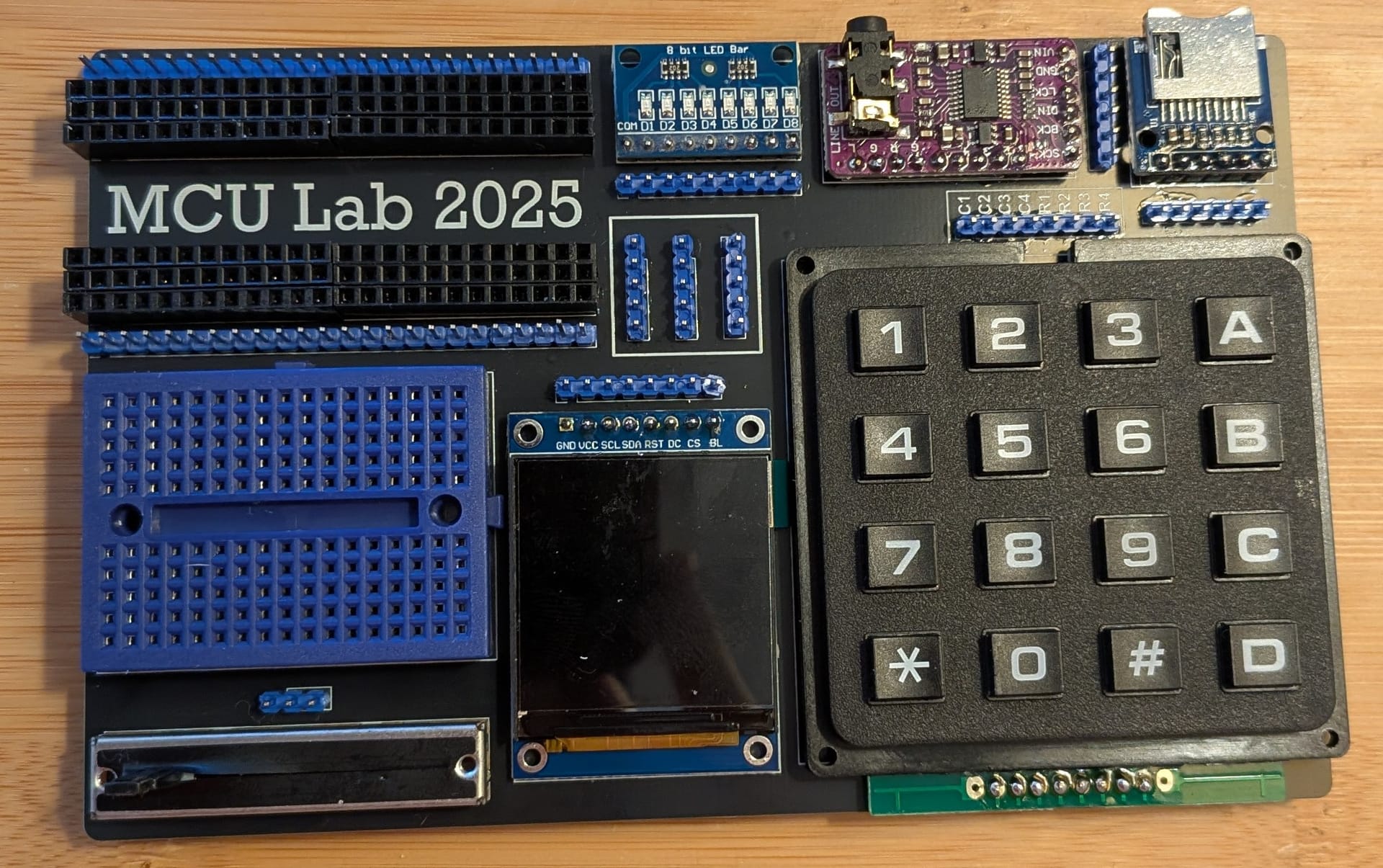
MCU Lab 2025
Its time to discern the transmundane again:
The MCU Lab is a compact development platform for prototyping and testing various microcontroller based designs. Six rows of 24 pin female headers comprise an MCU landing zone supporting the insertion of any DIP (dual inline package) format microcontroller development board having a width between 0.6 and 1.0 inches.
I see a dual inline package is a component for housing an integrated circuit, but more importantly there is the "JEDEC" standard that helps make it easy for everything to interoperate. The width is in reference to the distance between each pin in a row.
Also, its not super important for this box, but I realized that the pin numbering typically starts from the top left with pin 1, moves down, and then goes up the right side. The top is indicated by a little notch:
<a title="Licensing[edit]
Photo credit: Peter Halasz. (User:Pengo)
I, the copyright holder of this work, hereby publish it under the following license:
This file is licensed under the Creative Commons Attribution-Share Alike 3.0 Unported license.
You are free:
to share – to copy, distribute and transmit the work
to remix – to adapt the work
Under the following conditions:
attribution – You must give appropriate credit, provide a link to the license, and indicate if changes were made. You may do so in any reasonable manner, but not in any way that suggests the licensor endorses you or your use.
share alike – If you remix, transform, or build upon the material, you must distribute your contributions under the same or compatible license as the original.https://creativecommons.org/licenses/by-sa/3.0CC BY-SA 3.0 Creative Commons Attribution-Share Alike 3.0 truetrue
When employing the Creative Commons license, give attribution to:
Peter Halasz
and/or, link to this image page of Wikimedia Commons: http://commons.wikimedia.org/wiki/File:Pin_numbering_01_Pengo.svg
Although not a requirement of the license, if you use this image in print or media other than the web, I would appreciate it if you let me know. Please contact me if you require alternate licensing., CC BY-SA 3.0 <https://creativecommons.org/licenses/by-sa/3.0>, via Wikimedia Commons" href="https://commons.wikimedia.org/wiki/File:Pin_numbering_01_Pengo.svg">
The setup for the MCU Lab board is pretty slick: Components are soldered onto the board, along with pins. Traces on the board connect the components to the pins, but the components are not connected together. Instead I can use jumpers to connect the pieces as needed to experiment with the different MCUs.
This kit provides a lot of options for experimentation:
That also means a lot of soldering that needs to be done. Yes, I'm still trying to practice my soldering, but this seems like a monkey's paw moment. To give you an idea of how much soldering there was, I had to:
- Solder two 1x24 male headers into the "MCU Landing Zone" in the top left of the board.
- Solder 12 1x6 female headers into the landing zone.
- They note that "the two headers in each row should fit quite snuggly against each other". Most rows went in without issue for me. One was quite tricky.
- PCM5102A DAC
- Solder the four jumpers on the back of the board first. Since they cannot be accessed if the board is soldered down. See the audio section for a picture.
- Solder the 1x9 and 1x6 male header pins to the DAC board.
- Solder the board to the PCB.
- Solder the 1x6 male headers for jumpers to the MCU board.
- 4x4 matrix switch keypad
- The keypad has 10 pin holes, but the PCB only has 8. The outer pins on each side can be ignored, so pin 1 and 10.
- Solder the 1x8 male header to the keypad. Make sure to not position the header like normal. Instead of positioning the plastic between the PCB and the keypad, insert the longer pins into the PCB and solder them in place.
- Solder the keypad to the pins. There are plastic risers on the keypad for separation and this will make the keypad feel more sturdy.
- Solder the 1x8 male header for the jumpers to the MCU board.
- Color TFT LCD display
- Similar to the keypad, solder the 1x8 male header to the MCU board with the long pins sticking through. See below for a photo of how the pins are inserted.
- Then solder the display to the long pins. This will help the display sit flat.
- Above the board, solder the 1x8 male header for the jumpers onto the board.
- SD card slot
- Solder the 1x6 male header to the SD card slot. Note: I did this upside down. You should instead solder the board with the SD card on the underside. That way the pin numbering lines up with the jumper pins rather than being mirrored.
- Solder the SD card board to the MCU board.
- Solder the 1x6 male header for jumpers to the MCU board.
- Solder the 9 pins on the 8 Bit Blue LED Module to the top of the board.
- Add the three sets of 1x5 male headers to the middle of the PCB.
- Solder the three pins on the 100K Ohm Slide Potentiometer onto the board. I saved this for last since the slider is long and would make soldering the other pieces awkward.
Also each of the 4 MCUs needed to have their headers soldered on.
Phew!
The matrix keypad
This is my first time working with a keypad like this! It connects through 8 pins: C1-C4 and R1 to R4. As expected the C pins are for the columns and the R pins are for the rows.
The guide notes this pinout is setup for the ESp32, but can work with the other MCUs by changing the pin numbers, though doesn't clarify how. The example uses this Keypad library. The code sets up a 4x4 char array that maps each button to a specific character.
I wanted to know how this all works under the hood though. Here is a nice written guide that walks through how a membrane keyboard works with pictures, this guide talks about some of the details like timing and debounce, and this video is a useful visualization.
Essentially,
- The buttons are switches, like a membrane switch.
- The buttons in each column are connected to a shared trace that is exposed as a pin.
- Likewise the switches in each row have their own trace and pin.
- When a button is pressed, the trace for that button's row and column are connected.
- When the keypad is used with an MCU, the column pins are held high and the row pins are held low.
- Then when a button is pressed, the circuit is connected and the column pin is pulled low. That lets the MCU know what column was pressed.
- To get the row the MCU does a matrix scan and holds each column high one at a time. If any of the rows read high then that row is the correct column.
Its cool to finally learn how keypads actually work. I have used many mechanical keyboards, but I always buy them. The next time my keyboard dies I'm planning to build one instead. So this guide provided some nice background knowledge on the basics. Oh, also my friend is designing a phone/travel thumb keyboard and now maybe I can actually understand the project a bit.
The ST7789V Display
The first time I used a display was in box 0119 - Geopositioning which used a Adafruit ILI9341. This time the display is different:
- Last time the screen was 240x320, this time it is 240x240, so I have a new aspect ratio.
- The screen is physically smaller, 1.54 Inch instead of 2.8.
- The screen is color instead of black and white.
- The new screen is not touch sensitive.
- There is no build in SD card slot this time.
- This display uses the ST7789V driver chip instead of the ILI9341.
Here is a photo showing how to solder the pins for this board, as mentioned in the previous section:
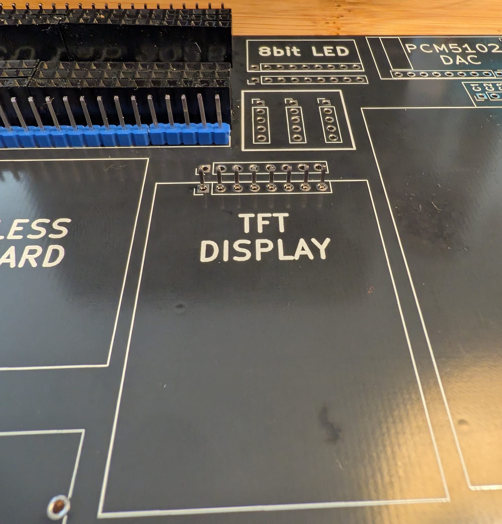
You need to install the Adafruit ST7735 and ST7789 library. The instructions note the screen will appear upside down and to use tft.setRotation(2); after setup, but doesn't provide an explanation why. I believe this is because by default the display is designed to have the pins on the bottom, but in our case we have it oriented the other way to make the traces to the pins easier.
SD card slot
The guide itself doesn't have much to say about the SD card.
In my write-up on the scanner prototype I talk about using SPI to write to an SD card. The process for setup in this guide is very similar so I won't go into the details too much. In fact the setup here is even simpler because we can use HSPI instead of VSPI. So we do not need the work around I had to use in my post.
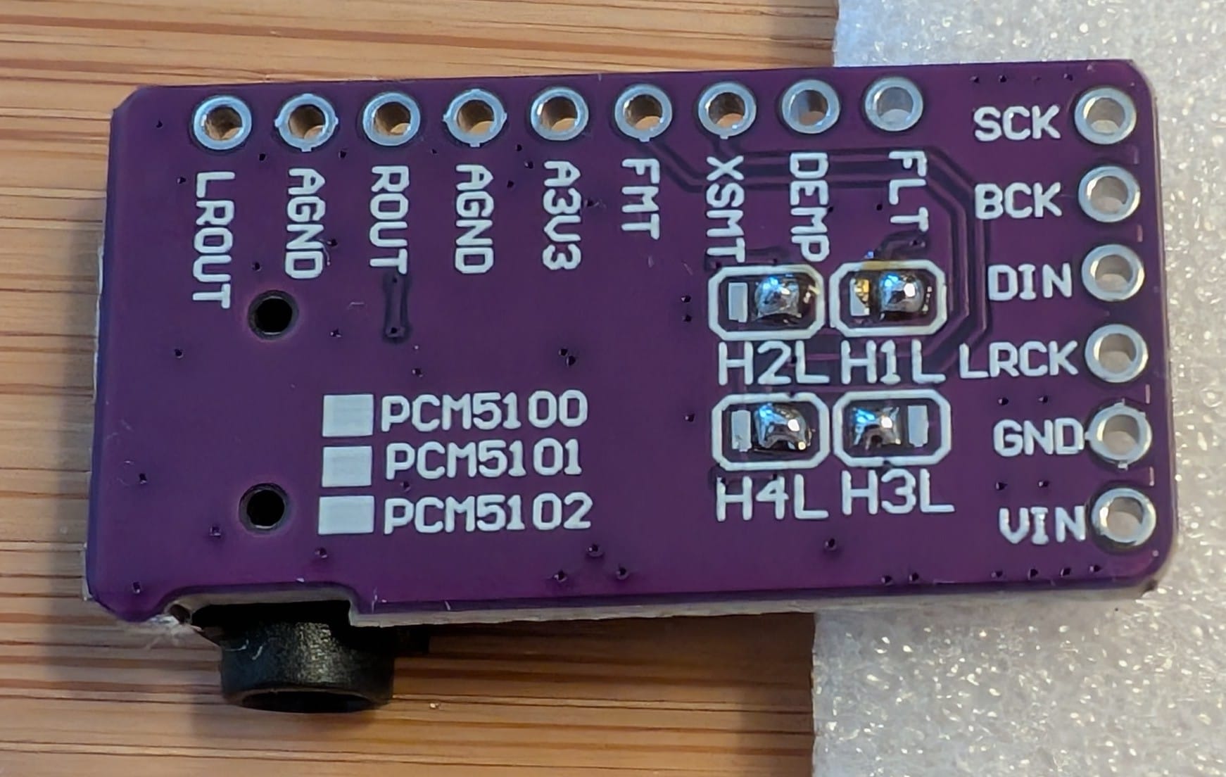
More audio experiments
PCM5102A is a stereo audio DAC. The board has four jumpers on the back that need to be solder to connec them:
- Jumper 3 is set HIGH
- Jumpers 1, 2, and 4 are set LOW
They don't explain why in the guide, so I went to read the datasheet, but realized that only covered the chip itself and not the breakout board. The jumpers are labeled H1L H2L H3L H4L and after digging for info on those its looks like the kit uses the GY PCM5102 DAC module. I found this helpful discussion thread about the jumpers which uses the same configuration with only H3L high and provides the explanation. There are screenshots to something, but with no link to the source. I've created the table here for better readability:
| H | Name | Description | LOW(GND) | HIGH(D 3.3V) |
|---|---|---|---|---|
| H1L | FLT | Filter Select | Normal latency | Low Latency |
| H2L | DEMP | De-emphasis control for 44.1kHz sampling rate | Off | On |
| H3L | XMST | Soft mute control | Soft Mute | Soft un-mute |
| H4L | FMT | Audio format selection | I2S | Left justified |
A wonderful, beautiful old fashion forum post from 2013 on diyAudio provided some context.
So putting that all together:
- Use normal latency mode. It looks like low latency mode is typically only used in studio editing applications.
- Some old CDs had pre-emphasis where weaker frequencies were boosted and would be de-emphasized during playback. This would improve signal-to-noise ratio. We are not using any audio with pre-emphasis so this is not needed.
- The "soft" part means that muting / unmuting is gradual rather than immediate. This helps reduce popping
- Use I2S for the audio format, similar to what I did in box 0118 More Human with the INMP441 microphone.
Also, I've never soldered jumper pads before and sparkfun had a nice guide that was helpful. Here is how they look soldered:
Outside of that the guide includes three audio experiments:
- Connect to WiFI, stream an mp3 of a DEFCON 2025 recording.
- Read an mp3 file off of the SD card.
- Setup the board as a Bluetooth audio device to stream music. This one was really cool.
A single sketch is used for all three experiments, commentinging/uncommenting lines as needed. The ESP32-audioI2S does a lot of the heavy lifting, which is nice, but obscures what is actually happening. Also, all three experiments use the ESP32, so using the other MCUs is left as an exercise to the reader.
Closing thoughts
The remainder of the guide talks a bit about cyberpunk literature and careers in embedded systems. I mostly glossed over those sections.
On the whole, I really liked this months box. I'd say this one is more potential, rather than hands on activities. I now have a lot of options to play with, which means this box will be used more often in the future than the one off projects in past boxes.
Member discussion